Laser Scribing for Wafer ID
MPE, Inc. operates fiber laser systems for scribing text on silicon wafers and other semiconductor wafers. Laser scribe is also referred to as laser marking, laser scribing, laser engraving, and serialization. Laser scribe service is often needed by wafer resizing customers. For example, a 200mm wafer may have its wafer ID text at the edge of the wafer, near the notch. The original wafer ID text will not be retained on a 150mm wafer that is cored from the center of the 200mm wafer. MPE can re-scribe the 150mm wafer to preserve identification and traceability.
In addition to providing laser scribe service for wafer resizing customers, MPE can provide laser scribe as a standalone service.
Capabilities
The following are our laser scribe capabilities:
- Laser scribe with the industry-standard SEMI OCR (optical character recognition) font as specified by the SEMI M12/M13 standard.
- Text can be scribed at any location on either side of the wafer.
- Text can be scribed on blank areas or onto existing patterning or circuits.
- Location and orientation can be optimized to fit text in tight areas outside functional die.
- Laser scribe can penetrate any existing protective photoresist or protective coating to leave legible text that is present after the coating is removed.
- Character height and dimensions are customizable. 2mm character height is standard.
- Laser power is kept low to minimize material removal and damage.
- MPE can transpose existing wafer ID to downsized wafer. Alternatively, customer may supply any custom ID text.
- Checksum characters can be generated per SEMI M12/M13 algorithm.
For any additional questions about our laser scribing services, please call us at 1-877-MPE-DICE, contact us via email, or fill out the request a quote form.
Laser Scribe: Front Side
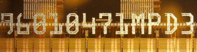
Pictured above is a wafer ID marked by MPE on the device side of a 150mm silicon CMOS wafer. MPE located the scribe on a partial die near the edge of the 150mm wafer. Device side (also known as frontside) scribes are used in many applications and are particularly useful for retaining identification when the backside of the wafer will eventually removed by a backgrind process.
Laser Scribe: Back Side
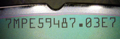
Pictured above is a 200mm silicon wafer with wafer ID text created by MPE’s laser scribe process. The scribe is located on the wafer backside, near the notch. Backsides scribes are useful to avoid consuming valuable space on the wafer’s device side, and backside scribes also offer excellent contrast.