Diagram 1 – 300mm wafer resized to various sizes.
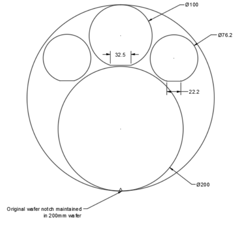
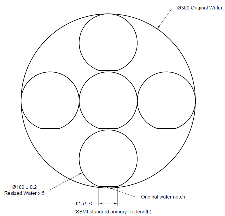
Diagram 2 – 300mm wafer resized to 5 x 100mm wafers.
Producing Excellent Cuts
Our facility, located just northeast of Dallas, Texas, is 8,000 square feet and includes multiple rooms equipped to safely and efficiently process material. Each room has several ESD measures in place, including wrist straps, ESD mats, ionized work stations, and ESD dicing film (for all ESD-sensitive material). Our state-of-the-art equipment, coupled with our outstanding process knowledge and experience, allow us to produce excellent cuts with minimal chipping. Our unique low-stress wafer resizing process results in downsized wafers with beveled and rounded edges without degradation to materials near the edge. We can work with any size semiconductor manufacturing firm. For smaller semiconductor firms without an in-house dicing facility, we can take care of all your wafer dicing and resizing needs. For medium to large semiconductor manufacturing firms that just cannot keep up with their orders, we can help by taking care of your overflow or assisting with R&D projects.
For any additional questions about our wafer resizing services, please call us at 1-877-MPE-DICE, contact us via email, or fill out the request a quote form.